AKONIS
Fully automated SIMS for compositional measurement in the semiconductor fab
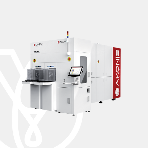
The AKONIS SIMS tool fills a critical gap in semiconductor fabrication processes by providing high throughput, high precision detection for implant profiles, composition analysis and interfacial data directly in the semiconductor manufacturing line. AKONIS offers a very high level of automation to ensure repeatability across tools for fab level process control and tool-to-tool matching.
AKONIS: SIMS Excellence Brought to the Fab!
Complementing the IMS Wf/SC Ultra as well as the SIMS 4550 (quadrupole SIMS) used to support the semiconductor industry via characterization labs, AKONIS – with full automation of instrument set-up and acquisition routines – enables rapid, within-fab analysis without compromise in analytical sensitivity. AKONIS benefits from recent development in EXtremely Low Impact Energy (EXLIE) ionic column technology (< 150 eV), coupled with a full wafer handling system including a high resolution stage enabling measurements on pads down to 20 μm.
The high yield enabler on N5 and beyond
- High resolution composition and fast dopant depth profiling of SiGe and SiP multilayer stacks
- Unrivalled in pad detection limits down to 20 μm
- More than 97% of time reduction to feedback data to the process line
- Blanket and patterned full wafer measurement
- Pattern recognition engine coupled with high resolution interferometric stage for < 2 μm position accuracy
- Intuitive recipe creation based on unique material database
- SEMI certified (S2/S8, E4, E5, E39, E84…)
- Low cost of ownership
For more information about this product, click here