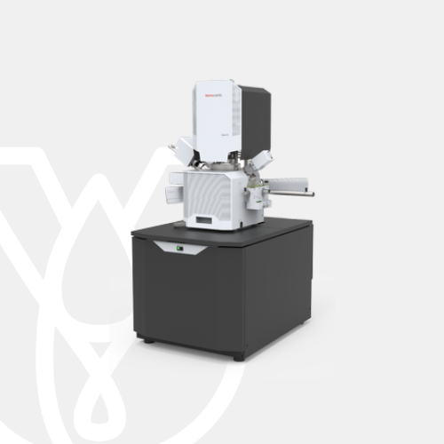
Apreo 2 SEM
PT Wadya Prima Mulia as the Authorized Distributor for ThermoFisher Scientific in Indonesia, provides Apreo 2 Scanning Electron Microscope
Scanning electron microscope for versatile, high performance materials imaging and analysis.
For more information regarding the product, click here
Materials characterization
Advanced materials characterization labs require access to the latest techniques and will push analytical tools, including SEMs, to the extremes of their capabilities. Most of these labs are multi-user facilities that accommodate users with varying degrees of experience. Time on the microscope is precious, and excessive time spent on maintenance, alignments, training, or image optimization needs to be avoided.
Apreo 2 Scanning Electron Microscope
The new Thermo Scientific Apreo 2 SEM expands access to high-performance imaging and analytics to all levels of microscopy expertise. With Thermo Scientific ChemiSEM Technology, a unique live elemental imaging capability, compositional information is always available, through the most intuitive interface. Eliminating all the hassle associated with typical EDS implementations, ChemiSEM Technology offers unprecedented time to result and ease of use.
The Apreo 2 SEM poses much smaller demands on users and lab managers with Thermo Scientific SmartAlign Technology, an optics system that aligns itself. Furthermore, the Apreo 2 SEM automates the image fine-tuning process with Thermo Scientific FLASH technology. FLASH Technology executes any necessary corrections to lens centering, the stigmators, and final focus of the image. The combination of these technologies means that users new to electron microscopy can access the high-end performance of the Apreo 2 SEM. Additionally, the Apreo 2 SEM is the only SEM with a 1-nanometer resolution at 10 mm analytical working distance. No longer does long working distance mean poor imaging. With the Apreo 2 SEM, anyone will be able to confidently get great results.
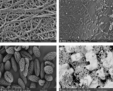
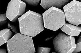
Excellent image quality
Excellent image quality at low kV and low vacuum thanks to flexible vacuum modes, including through-the-lens differential pumping. Simultaneous secondary electron (SE) and backscattered electron (BSE) imaging in every mode of operation.
In-situ study of materials in their natural state
With the Prisma E SEM’s environmental SEM (ESEM) mode, samples can be imaged even if they are hot, dirty, outgassing or wet.
Easy to use
Easy to use, intuitive software with user guidance and undo functionality makes highly effective operation possible for novice users, while enabling experts to do their work faster and with fewer mouse clicks.
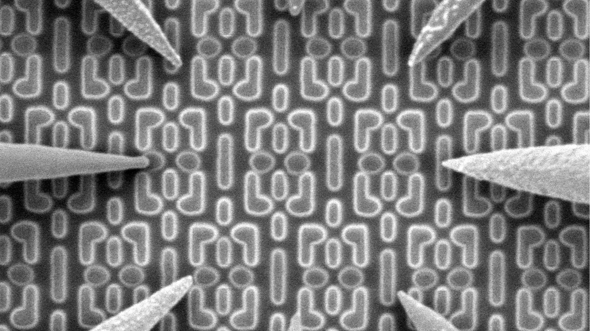
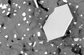
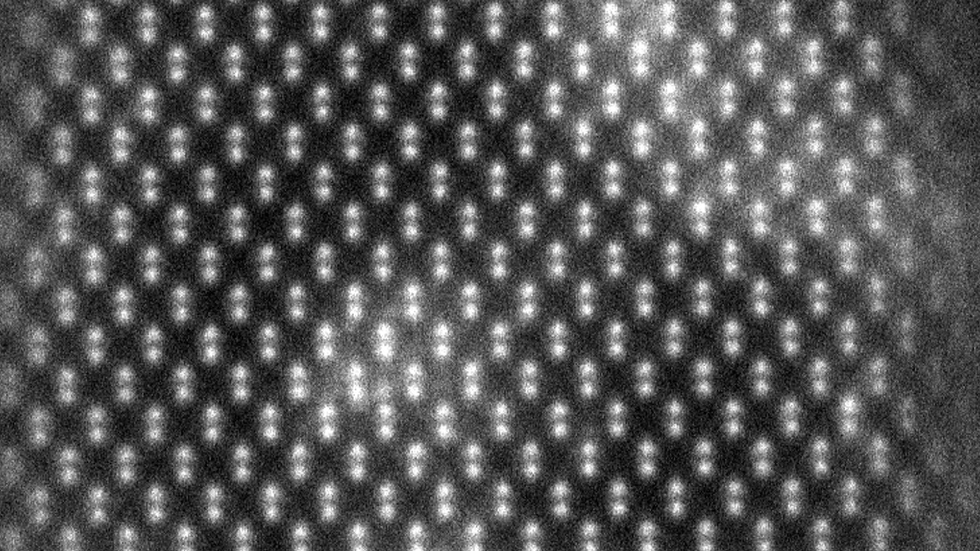
High performance, resolution, and contrast
The combination of advanced optics, detection and automation in Apreo 2 makes obtaining high resolution imaging possible even for users new to SEM

Wide range of sample types
Apreo 2 was designed for maximum flexibility. High quality, high resolution imaging is possible regardless of target samples properties. Insulators, beam sensitive or magnetic materials can all be imaged with ease thanks to Apreo 2’s unique optics, detection and beam control options.
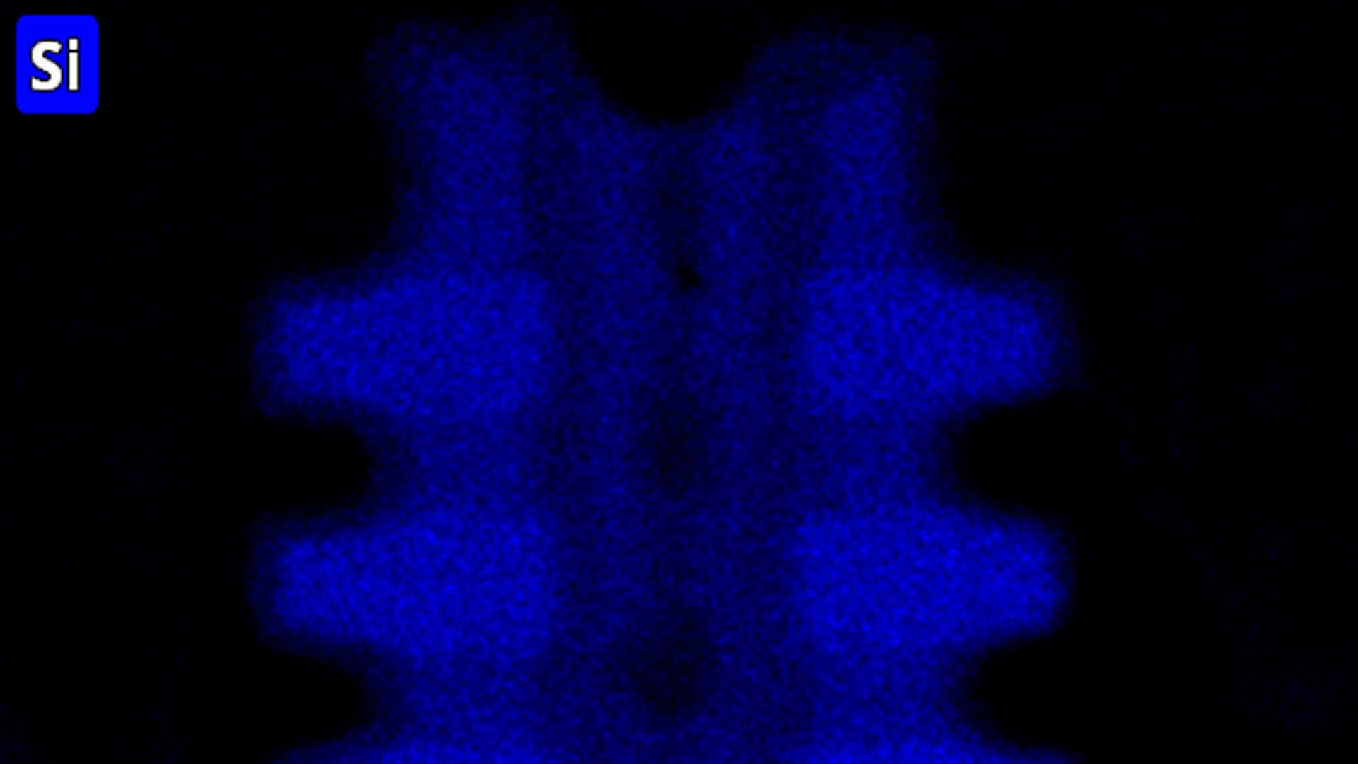
Live quantitative EDS with ChemiSEM
Elemental information at your fingertips with ChemiSEM, which provides live quantitative elemental mapping for unprecedented time to result and ease of use.
Quick and easy sample loading
Easy access to the stage, a convenient multi-sample holder, and a fast pump down ensures no time is wasted loading samples. An automated routine to insert and remove a pressure limiting aperture (PLA) allows for a seamless switch between high and low vacuum without opening the chamber.
Advanced automation
From optics, to image acquisition, Apreo 2 provides a range of automated features to make imaging time as effective and efficient as possible. Flash Technology automates image fine tuning The unique Undo function permits efficient exploration of imaging conditions Thermo Scientific Maps software automates large area acquisition with up to 4 different simultaneous signals
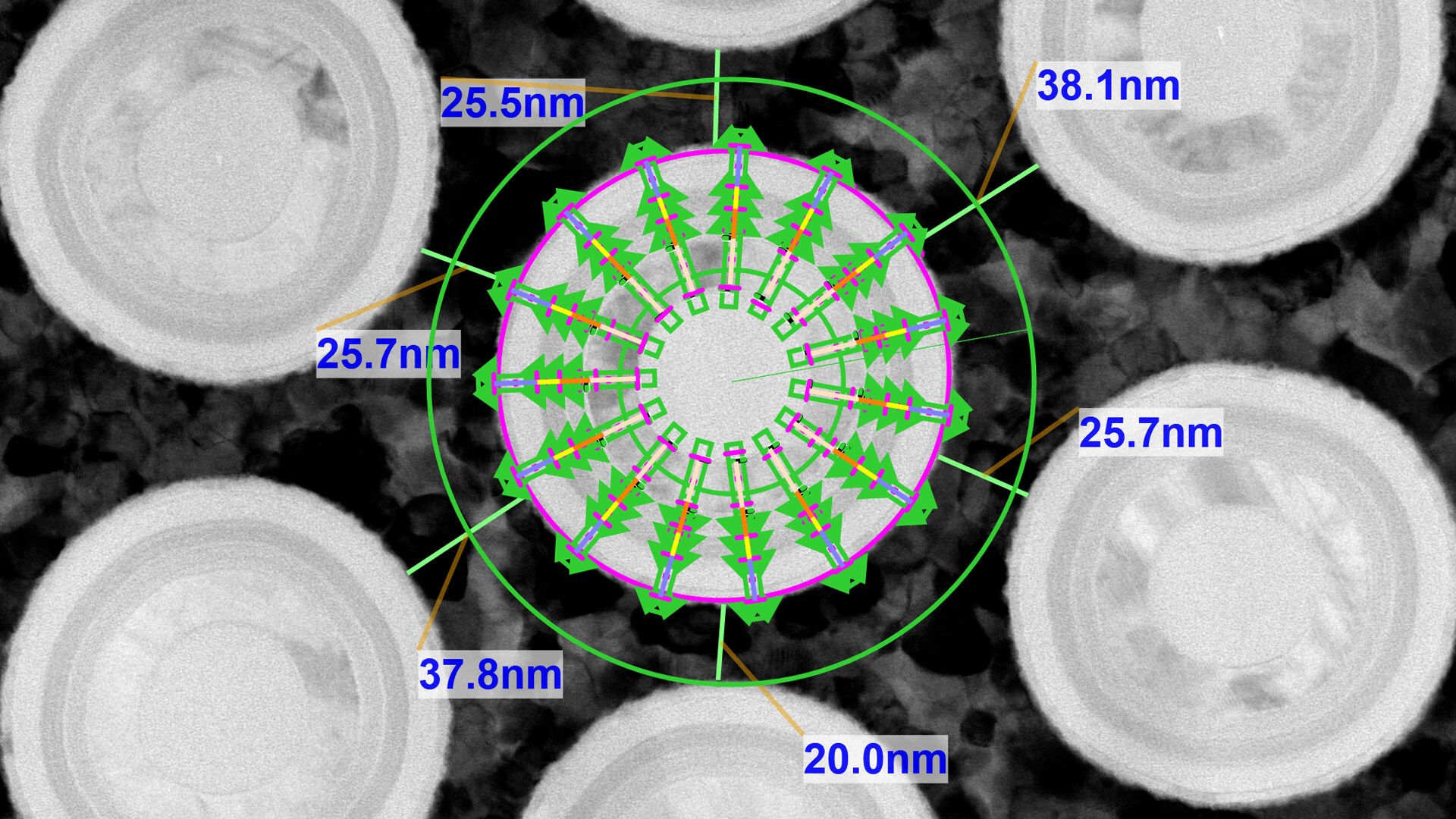
Performance at long working distance
Apreo 2 is the only SEM that offers high-resolution performance (1nm) and excellent image quality at analytical working distance (10mm). Sample morphology, topography and surface information can all be simultaneously explored while being at a safe distance from the pole piece. Thanks to its high-speed and high-sensitivity in-lens backscattered detector, BSE are still detected even at extremely low beam currents (as low as few pA).
| Resolution | • 0.9 nm at 1 kV • 0.8 nm at 1 kV (beam decel.) • 1.0 nm at 1 kV, 10 mm working distance (beam decel.) • 0.8 nm at 500 V (beam decel.) • 1.2 nm at 200 V (beam decel.) |
| Standard detectors | ETD, T1, T2, T3, IR-CCD, Nav-Cam+ |
| PivotBeam | Mode for selected area electron channeling (also known as “rocking beam” mode). |
| Optional detectors | DBS, LVD, DBS-GAD, STEM 3+, RGB-CLD, EDS, EBSD, WDS, Raman, EBIC, etc. |
| ChemiSEM Technology (optional) | Live quantitative SEM image coloring is available based on energy dispersive X-ray spectroscopy (EDS). Point & ID, linescan, region, element maps, and reliable Noran quantification are included. |
| Landing energy range | 20 eV – 30 keV |
| Stage bias (beam deceleration, optional) | -4000 V to +600 V standard with every system |
| Low vacuum mode | Optional: 10 – 500 Pa chamber pressure |
| Stage | 5-axis motorized eucentric stage, 110 x 110 mm2 with a 105° tilt range. Maximum sample weight: 5 kg in un-tilted position. |
| Maximum beam current | 50 nA (400 nA configuration also available) |
| Standard sample holder | Multi-purpose holder, uniquely mounts directly onto the stage, hosts up to 18 standard stubs (Ø12 mm), three pre-tilted stubs, cross-section samples and two pre-tilted row-bar holders (38° and 90°) and does not require tools to mount a sampl |
| Chamber | 340 mm inside width, 12 ports, three simultaneous EDS detectors possible, two at 180°, coplanar EDS/EBSD orthogonal to the tilt axis of the stage |
Semiconductor Failure Analysis
Complex semiconductor device structures result in more places for defects to hide. Learn more about failure analysis solutions to isolate, analyze, and repair defects.
Quality control and failure analysis
Quality control and assurance are essential in modern industry. We offer a range of EM and spectroscopy tools for multi-scale and multi-modal analysis of defects, allowing you to make reliable and informed decisions for process control and improvement.
Fundamental Materials Research
Novel materials are investigated at increasingly smaller scales for maximum control of their physical and chemical properties. Electron microscopy provides researchers with key insight into a wide variety of material characteristics at the micro- to nano-scale.
Semiconductor research and development
Innovation starts with research and development. Learn more about solutions to help you understand innovative structures and materials at the atomic level.
Manufacturing today’s complex semiconductors requires exact process controls. Learn more about advanced metrology and analysis solutions to accelerate yield learnings.
Semiconductor materials characterization
Many factors impact yield, performance, and reliability. Learn more about solutions to characterize physical, structural, and chemical properties.

Semiconductor display technology
Display technologies are evolving to improve display quality and light conversion efficiency. Learn how metrology, failure analysis, and characterization solutions provide insights.
For other products from ThermoFisher, click here.