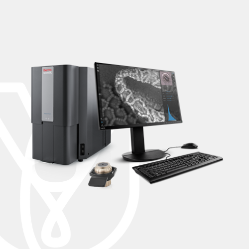
PT Wadya Prima Mulia as the Authorized Distributor for ThermoFisher Scientific in Indonesia, providesPhenom ProX Desktop Scanning Electron Microscope
Desktop SEM with EDS capability for robust, effortless, and versatile elemental and SEM analysis.
For more information regarding the product, click here
Phenom Desktop SEM with energy-dispersive X-ray diffraction
The sixth-generation of Thermo Scientific Phenom ProX G6 Desktop SEM fills the gap between light microscopy and floor-model SEM analysis, thus expanding the capabilities of research facilities. It offers fast, high-resolution imaging in addition to an integrated energy-dispersive X-ray diffraction (EDS) detector for robust, easy-to-use, rapid elemental analysis.
Fast and easy to use
The Phenom Pro Desktop SEM can be used to relieve the burden of routine analysis for common samples from floor-model SEM instruments. Instrument configuration and the sample loading mechanism ensure quick imaging with minimal time spent tuning between experiments.
Long-lifetime CeB6 source
Facility users of any experience level can quickly begin producing high-quality results with the Phenom Pro Desktop SEM. Its long-lifetime CeB6 source offers high brightness while requiring low maintenance.
Robust and small form factor
It’s high stability and small form factor allow the instrument to be used in practically any lab environment; more simply put, it does not require specialized infrastructure or expert oversight.
| Light optical magnification | 27–160x |
| Electron optical magnification range | 160-350,000x |
| Resolution | ≤ 6 nm SED and ≤ 8 nm BSD |
| Digital zoom | Max. 12x |
| Light optical navigation camera | Color |
| Acceleration voltages | • Default: 5 kV, 10 kV and 15 kV • Advanced mode: adjustable range between 4.8 kV and 20.5 kV imaging and analysis mode |
| Vacuum modes | • High vacuum mode • Charge reduction mode via optional low vacuum sample holder |
| Detector | • Backscattered electron detector (standard) • Energy-dispersive X-ray detector (standard) • Secondary electron detector (optional) |
| Sample size | Up to 25 mm diameter (optional 32 mm) |
| Sample height | Up to 35 mm (optional 100 mm) |
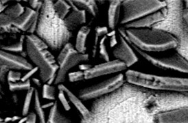
Process control using electron microscopy
Modern industry demands high throughput with superior quality, a balance that is maintained through robust process control. SEM and TEM tools with dedicated automation software provide rapid, multi-scale information for process monitoring and improvement.
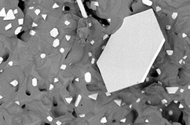
Quality control and failure analysis
Quality control and assurance are essential in modern industry. We offer a range of EM and spectroscopy tools for multi-scale and multi-modal analysis of defects, allowing you to make reliable and informed decisions for process control and improvement.
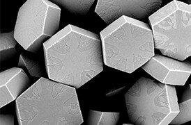
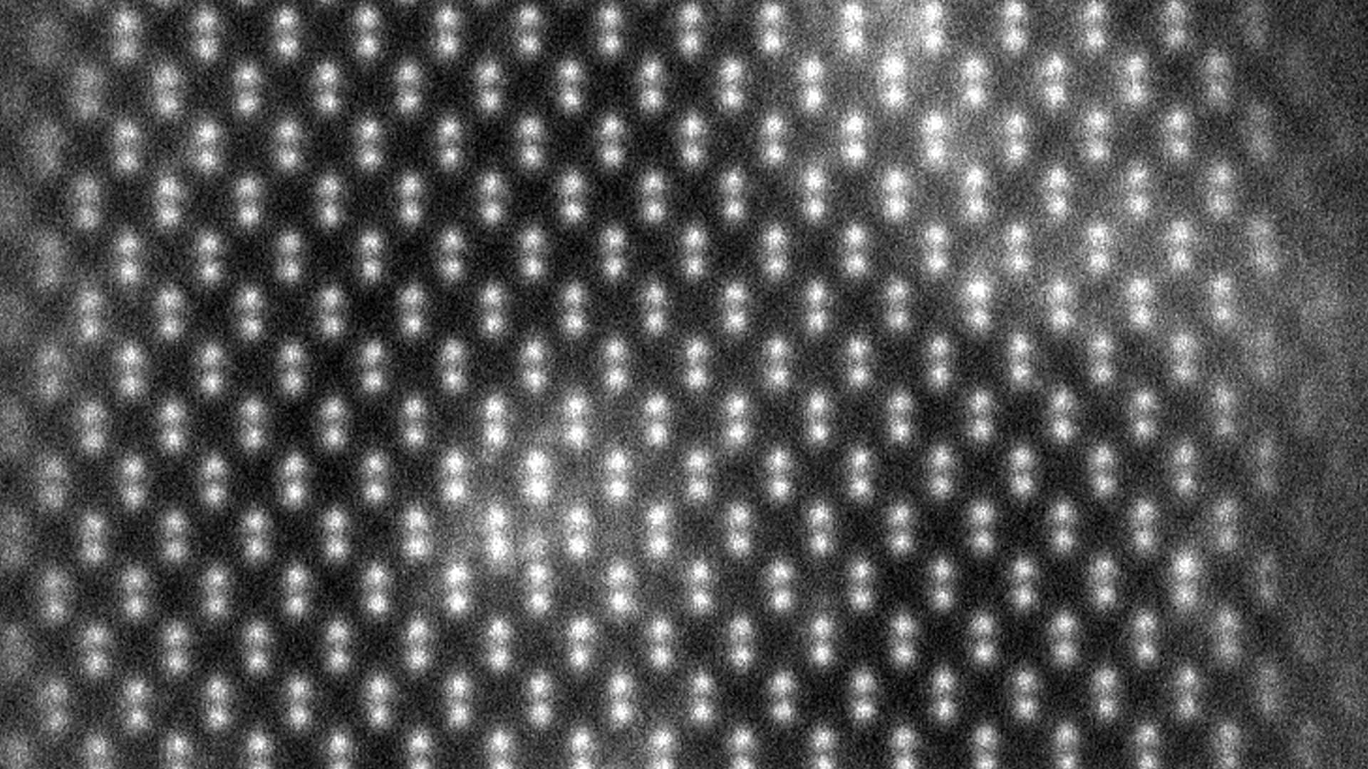
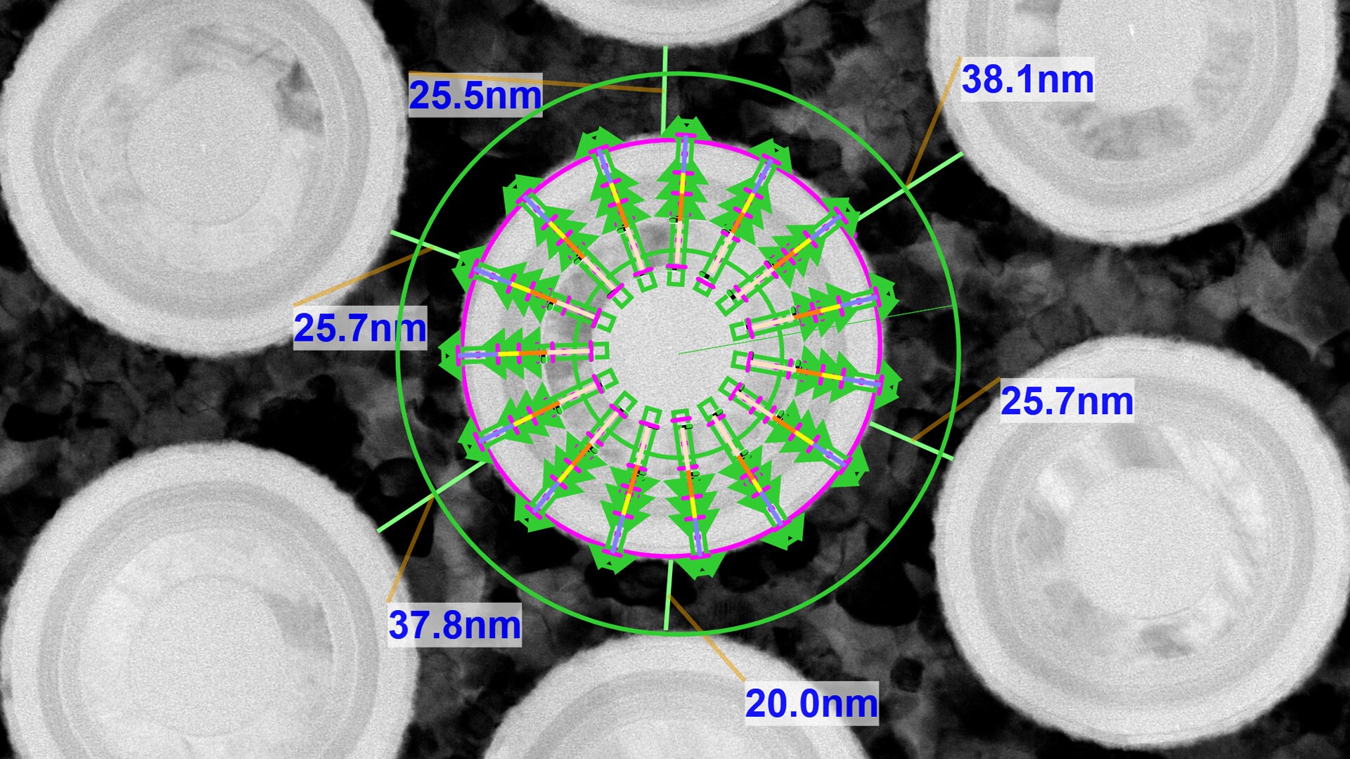
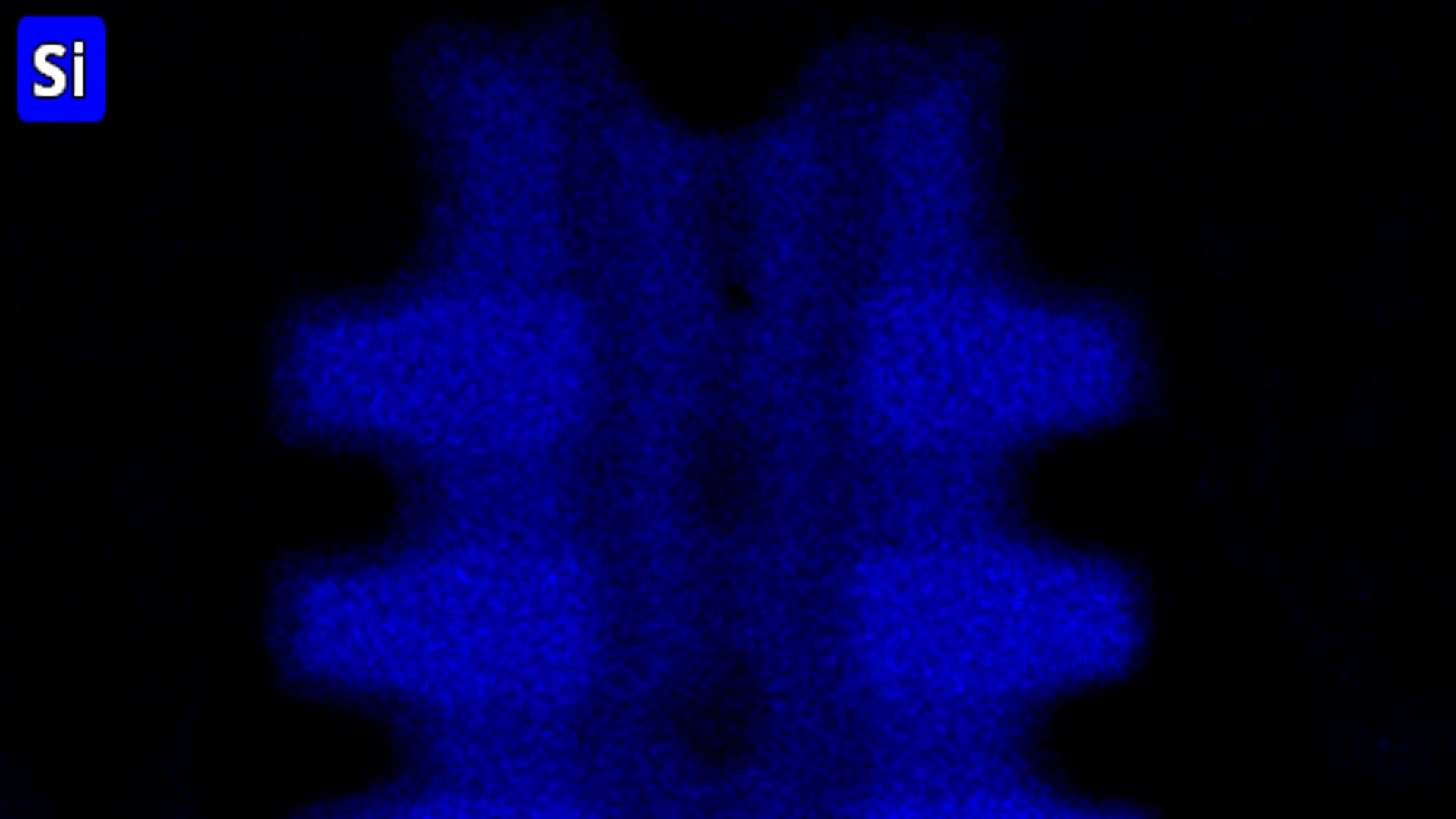
Fundamental Materials Research
Novel materials are investigated at increasingly smaller scales for maximum control of their physical and chemical properties. Electron microscopy provides researchers with key insight into a wide variety of material characteristics at the micro- to nano-scale.
Semiconductor research and development
Innovation starts with research and development. Learn more about solutions to help you understand innovative structures and materials at the atomic level.
Manufacturing today’s complex semiconductors requires exact process controls. Learn more about advanced metrology and analysis solutions to accelerate yield learnings.
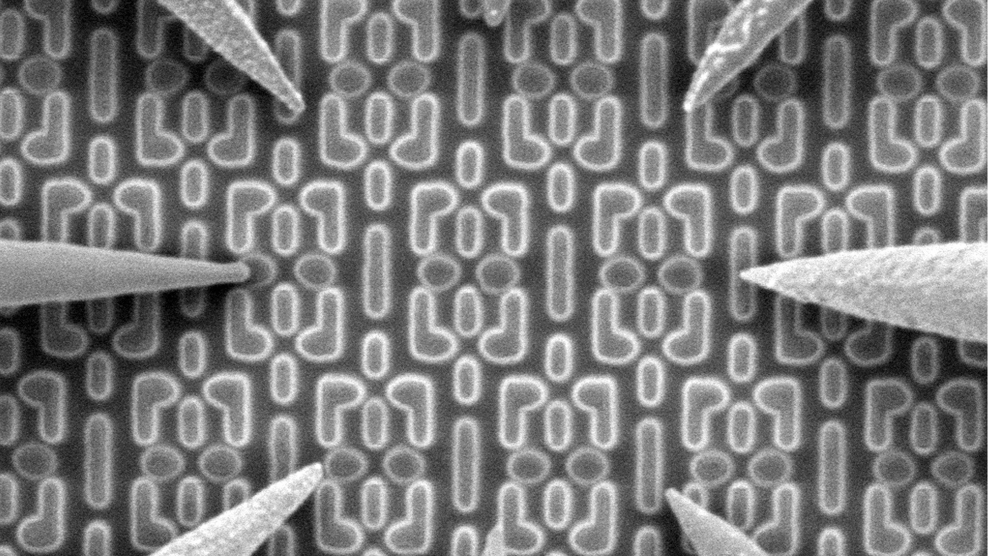
Semiconductor Failure Analysis
Complex semiconductor device structures result in more places for defects to hide. Learn more about failure analysis solutions to isolate, analyze, and repair defects.
Semiconductor materials characterization
Many factors impact yield, performance, and reliability. Learn more about solutions to characterize physical, structural, and chemical properties.
For other products from ThermoFisher, click here.