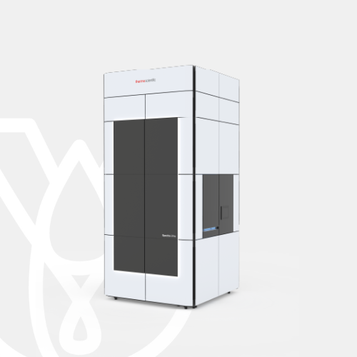
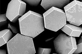
PT Wadya Prima Mulia as the Authorized Distributor for ThermoFisher Scientific in Indonesia, provides Spectra Ultra Scanning Transmission Electron Microscope
Scanning transmission electron microscope for imaging and spectroscopy of beam sensitive materials.
For more information regarding the product, click here
Spectra Ultra Scanning Transmission Electron Microscope
To truly optimize TEM and STEM imaging, EDX and EELS may require acquisition of different signals at different accelerating voltages. The rules may vary from sample to sample but, it is generally accepted that: 1) the best imaging is done at the highest possible accelerating voltage above which visible damage will occur, 2) EDX, especially when mapping, benefits from lower voltages with increased ionization cross-sections, thus yielding better signal-to-noise ratio maps for a given total dose, and 3) EELS works best at high voltages to avoid multiple scattering, which degrades the EELS signal with increasing sample thickness.
Unfortunately, acquisition at different accelerating voltages on the same sample without losing the region of interest—all during a single microscopy session—is not possible. At least, until now.
Imagine a Thermo Scientific Spectra 300 S/TEM:
- That can truly be operated at different voltages (all the voltages between 30 and 300 kV for which alignments were purchased) in a single microscopy session
- Where changing from an accelerating voltage to any other one takes about 5 minutes
- That can accommodate a radically different EDX concept with a 4.45 srad solid angle (4.04 srad solid angle with an analytical double tilt holder)
With the new Spectra Ultra S/TEM, the accelerating voltage becomes an adjustable parameter, just like probe current, and the massive Ultra-X EDX system enables chemical characterization of materials too beam-sensitive for conventional EDX analysis.
The Spectra Ultra aberration-corrected S/TEM offers an industry leading level of characterization capabilities for materials science and semiconductor applications at the highest resolution on a wide variety of samples.
Built on an ultra-stable foundation
The Spectra Ultra S/TEM is delivered on a platform designed to offer an unprecedented level of mechanical stability quality through passive and (optional) active vibration isolation.
Like the Thermo Scientific Spectra 200 S/TEM and Spectra 300 S/TEM, the system is housed in a fully redesigned enclosure with a built-in on-screen display for convenient specimen loading and removal. For the first time, full modularity and upgradeability can be offered between uncorrected and single-corrected configurations with variable heights, allowing maximum flexibility for different room configurations.
Fastest time to optimized results from more materials
The ability to switch accelerating voltage and achieve ultimate stability of the optics and specimen stage in less than five minutes provides unique capabilities and a new, faster way to operate the microscope to extract optimized information from your specimen.
- The highest resolution spatial information (50 pm) from a specimen can be collected at 300 kV. Then, the system can be switched to lower accelerating voltages for STEM EDX mapping with increased ionization cross sections from the same area with higher X-ray yields, leading to reduced sample damage.
- For specimens that suffer from “knock-on” damage, the accelerating voltage can be switched multiple times within a single microscopy session to mitigate beam damage and ensure data integrity is maintained.
This capability is achieved by the introduction of a radically redesigned objective lens that can operate at constant power for all accelerating voltages between 30 and 300 kV.

The constant power concept was pioneered with the introduction of the Titan TEM, formerly produced by FEI, over a decade and a half ago. It enabled mode switching at any given, but fixed, accelerating voltage without inducing drift because the objective lens thermal load would remain constant. Now, this concept has been extended to all voltage changes between 30 and 300 kV.
The objective lens produces magnetic fields that vary wildly depending on the mode and accelerating voltage. However, for the Spectra Ultra (S)TEM’s new objective lens, the thermal load remains constant at all times. The stabilization time of the optics and stage when switching between different accelerating voltages has been reduced from several hours to less than five minutes.
The benefits of accelerating voltage flexibility in combination with the Ultra-X detector are clear. Fast and flexible control over the HT, in combination with Ultra-X, opens the gateway to fast imaging at the highest resolution in combination with optimized STEM EDX analysis of beam-sensitive materials.
Lowest dose STEM/EDX for the characterization of more materials
The Spectra Ultra S/TEM brings the next era in EDX detection to the market with our Ultra-X EDX detector. Providing a solid angle (>4.45 Sr) at least two times greater than any other EDX detector solution, the sensitivity of Ultra-X opens up new capabilities in STEM EDX analysis. Even with the shadowing of an analytical double tilt holder considered, the solid angle is >4.04 srad

Additionally, the high sensitivity of Ultra-X means that the same level of chemical information can be obtained with a fraction of the electron dose that would be required for other EDX detector solutions. This opens up possibilities for STEM EDX analysis from more beam-sensitive specimens and faster mapping for more stable specimens.

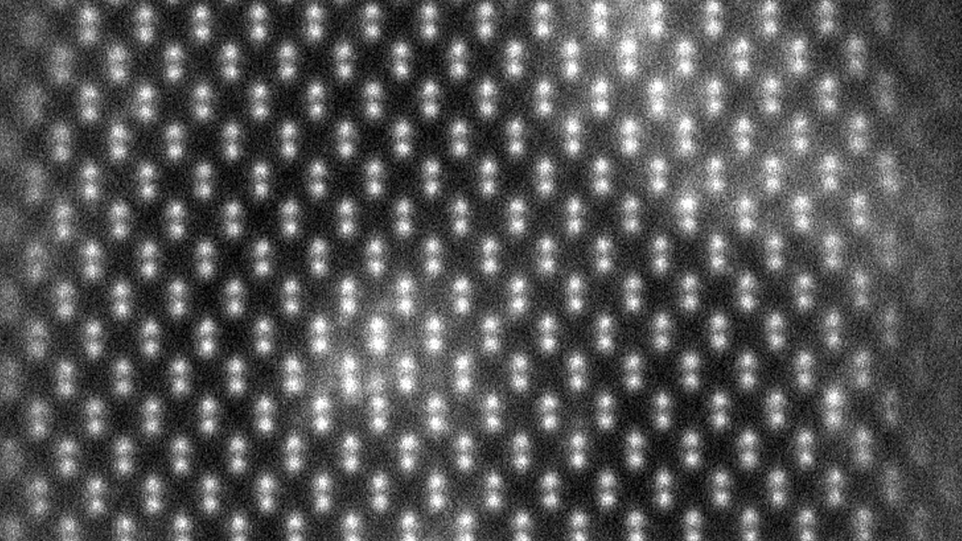
The benefits of such high sensitivity are shown in the improvement in spectrum imaging quality with Ultra-X. A comparison using the same electron dose (8.28 x 10⁸ e/Å2) is shown between Super-X, Dual-X, and Ultra-X on a DyScO3 specimen. The improvements in the signal-to-noise ratio shown in the raw data can be easily seen. Additionally, the oxygen lattice can be directly imaged with Ultra-X, where it could not with Super-X and Dual-X.

Unprecedented sensitivity with the Panther STEM detection system
STEM imaging on the Spectra Ultra S/TEM has been reimagined with the Panther STEM detection system, which includes a new data acquisition architecture and two new, solid-state, eight-segment ring and disk STEM detectors (16 segments in total). The new detector geometry offers access to advanced STEM imaging capability combined with the sensitivity to measure single electrons.

Scanning image of the 16 segmented ring and disk detectors with an intensity profile (in red) proving the excellent homogeneity of sensitivity across the segments.

Highest resolution STEM imaging performance
The Spectra Ultra S/TEM is equipped with the new S-TWIN’ (S-TWIN Prime) pole piece. The S-TWIN’ is based on the S-TWIN design. It provides both ultra-high spatial resolution in STEM (e.g., 50 pm at 300 kV and 96 pm at 60 kV) and a wide gap for experiments requiring large tilt angles or bulky in situ holders.
The S-TWIN’ differs in its ability to support an extremely high solid-angle EDX solution (see section on Ultra-X) without compromising spatial resolution. The S-TWIN’, in combination with the enhanced mechanical stability of the base and the latest S-CORR probe corrector, matches the combined spatial resolution and combined high probe current specifications of the Spectra 300 TEM.
High-energy resolution and high-brightness sources
X-FEG/Mono or X-FEG/UltiMono
The Spectra Ultra S/TEM can be optionally equipped with either a standard monochromator (X-FEG/Mono) or a high-energy resolution monochromator (X-FEG/UltiMono). Both monochromators are automatically excited and tuned with single-click operation to achieve the highest energy resolution possible on each configuration by using OptiMono or OptiMono+, respectively.
The X-FEG/Mono can be automatically tuned from 1 eV down to 0.2 eV, while the X-FEG/UltiMono can be automatically tuned from 1 eV down to <25 meV.
Both sources can be operated from 30 to 300 kV to accommodate the widest range of specimens. Both can also be run in standard mode, with the monochromators switched off, to accommodate experiments that require high brightness, including STEM EDS mapping, ultra-high-resolution STEM, or high total current, such as TEM imaging, all with no compromise to the other specifications of the system. This flexibility gives the Spectra Ultra (S)TEM the capability to function in settings where a large range of experiments are expected to be performed on one system.
X-CFEG
The Spectra Ultra S/TEM can optionally be powered by a new cold field emission gun (X-CFEG). The X-CFEG has extremely high brightness (>>1.0 x 10⁸ A/m2/Sr/V*), low energy spread (<0.4 eV), and can operate from 30 to 300 kV. This provides simultaneous high-resolution STEM imaging with high probe currents for high throughput, fast acquisition STEM analytics in parallel with high-energy resolution. With the powerful combination of X-CFEG and the S-CORR probe aberration corrector, sub-Angstrom (<0.8 Å) STEM-imaging resolution with over 1,000 pA of probe current can be routinely achieved.

Further, probe currents can be flexibly tuned from <1 pA up to the nA range with fine control of the gun and condenser optics, all with minimum impact on the probe aberrations, so that the widest range of specimens and experiments can be accommodated.
As with all cold field emission sources, the sharp tip requires a periodic regeneration (called flashing) to maintain the probe current. With the X-CFEG, the tip only requires flashing once per working day, a process takes less than a minute. There is no measurable impact on the probe aberrations even in the highest resolution imaging conditions, and the daily tip flashing process has no impact on the tip lifetime.
This new generation X-CFEG also produces enough total beam current (>14 nA) to support standard TEM imaging experiments (e.g. in situ) with large parallel probes, making it a uniquely all-purpose, yet high performance, C-FEG.
Adding to the flexible nature of the X-CFEG is the capability to adjust the energy resolution by varying the extraction voltage.
In the example below, the energy resolution was adjusted between 0.39eV, with <500pA of probe current and 0.31eV, with >300pA of probe current. Maintaining high probe currents with high energy resolution allows for detailed analysis of Energy Loss Near Edge Structure (ELNES) analysis without the need for a monochromator on core loss edges. The spatial resolution, as demonstrated in the HAADF image of DyScO3, remains unaffected (in this case <63pA) which means that STEM EELS experiments with simultaneously high spatial resolution, energy resolution and signal to noise ratio can now be performed.
The lifetime of the tip is unaffected by the extraction voltage chosen to perform the experiment.

Advanced STEM imaging capabilities
The Spectra Ultra S/TEM can be configured with an electron microscope pixel array detector (EMPAD) or a Thermo Scientific Ceta™ Camera with speed enhancement to collect 4D STEM data sets.
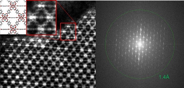
The EMPAD is capable of 30–300 kV and provides a high dynamic range (1:1,000,000 e- between pixels), high signal- to-noise ratio (1/140 e-), and high speed (1,100 frames per second) on a 128×128 pixel array, which makes it the optimal detector for 4D STEM applications (e.g., where the details of the central and diffracted beams need to be analyzed simultaneously, as in the following ptychography image).

In situ capabilities of the Spectra Ultra S/TEM
The Spectra Ultra S/TEM accepts a wide range of holders for in situ experiments with its all-in-one S-TWIN’ wide-gap pole piece. The family of Thermo Scientific NanoEx Holders can be seamlessly integrated with the microscope, enabling MEMS device-based heating for atomic imaging at elevated temperatures. Below, gold nanoparticles are heated to 700 degrees Celsius and the resulting motion is captured simultaneously with full frame 4k by 4k pixel resolution at a rate greater than 30 frames per second on a Ceta Camera with speed enhancement. The result is high spatial and temporal resolution of highly dynamic molecular behavior.
| Uncorrected | • Energy spread: 0.2–0.3 eV • Information limit: <100 pm • STEM resolution: <136 pm |
| Probe corrected | • Energy spread: 0.2–0.3 eV • Information limit: <100 pm • STEM resolution: <50 pm (125 pm @ 30 kV) |
| STEM resolution: <50 pm (125 pm @ 30 kV) | • Energy spread: 0.2–0.3 eV • Energy spread: 0.2–0.3 eV • STEM resolution: <50 pm at 300kV with >30pA of probe current STEM resolution: <125 pm at 30kV with >20pA of probe current |
| Probe+Image Corrected X-FEG/UltiMono | • Energy spread: 0.05 eV (0.025 eV @ 60kV) • Information limit: <60 pm • STEM resolution: <50 pm at 300kV >30pA of probe current STEM resolution: <50 pm at 300kV >30pA of probe current |
| Probe+Image Corrected X-CFEG | • Energy spread: 0.4 eV • Information limit: <70 pm • STEM resolution: <50 pm (<136 pm @ 30 kV) with >100pA of probe current |
| Source | • X-FEG Mono: High-brightness Schottky field emitter gun and monochromator with a tunable energy resolution range between 1 eV and <0.2 eV • X-FEG UltiMono: High-brightness Schottky field emitter gun with ultra-stable monochromator and accelerating voltage with a tunable energy resolution range between 1eV and <0.05 eV (<0.025eV @ 60kV) • X-CFEG: Ultra-high brightness with an intrinsic energy resolution of <0.4 eV with 14nA of total beam current and <0.3eV with 2nA of total beam current • Flexible high-tension range from 30 – 300 kV |
Process control using electron microscopy
Modern industry demands high throughput with superior quality, a balance that is maintained through robust process control. SEM and TEM tools with dedicated automation software provide rapid, multi-scale information for process monitoring and improvement.
Quality control and failure analysis
Quality control and assurance are essential in modern industry. We offer a range of EM and spectroscopy tools for multi-scale and multi-modal analysis of defects, allowing you to make reliable and informed decisions for process control and improvement.
Fundamental Materials Research
Novel materials are investigated at increasingly smaller scales for maximum control of their physical and chemical properties. Electron microscopy provides researchers with key insight into a wide variety of material characteristics at the micro- to nano-scale.
Semiconductor research and development
Innovation starts with research and development. Learn more about solutions to help you understand innovative structures and materials at the atomic level.
For other products from ThermoFisher, click here.