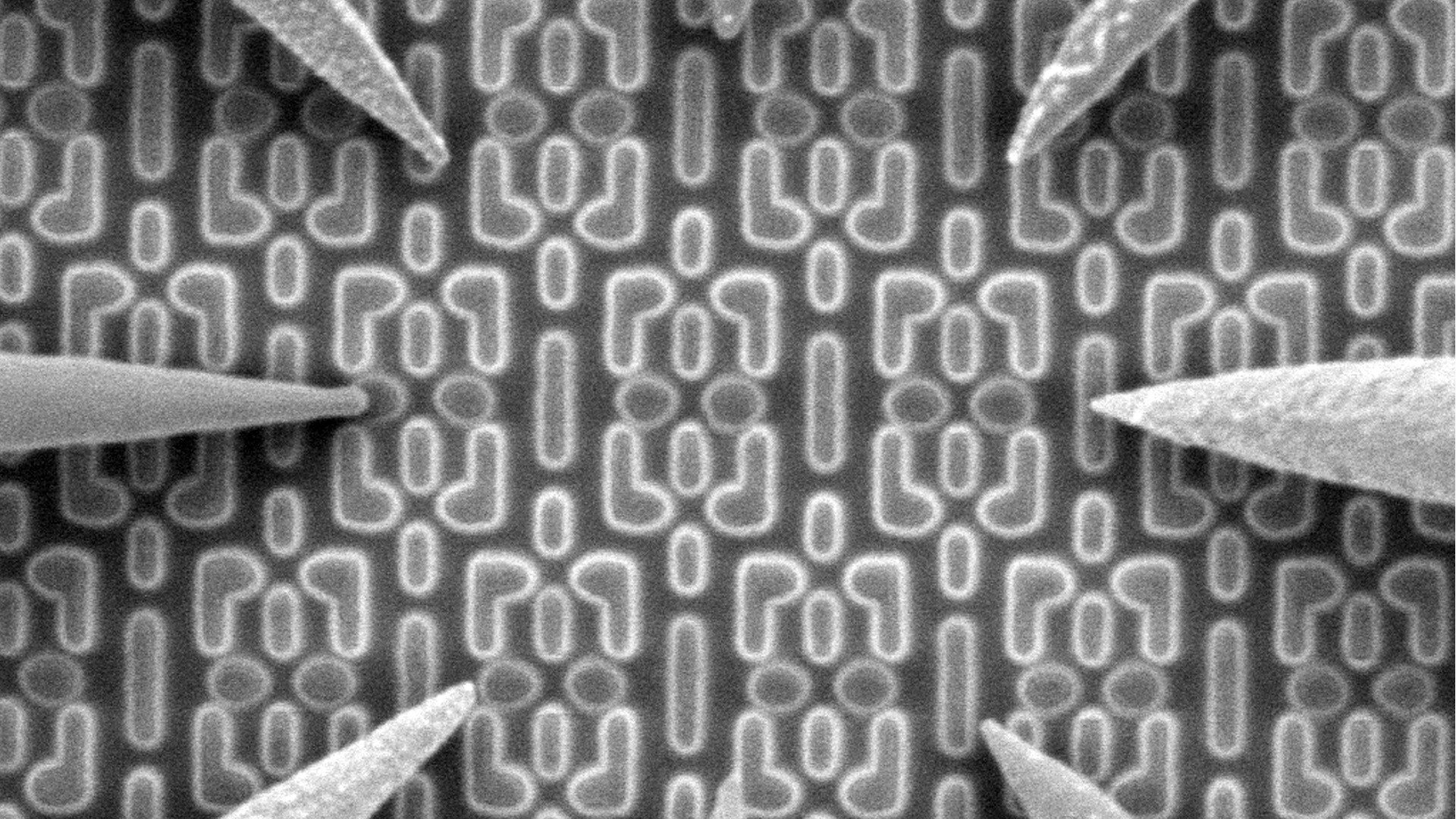
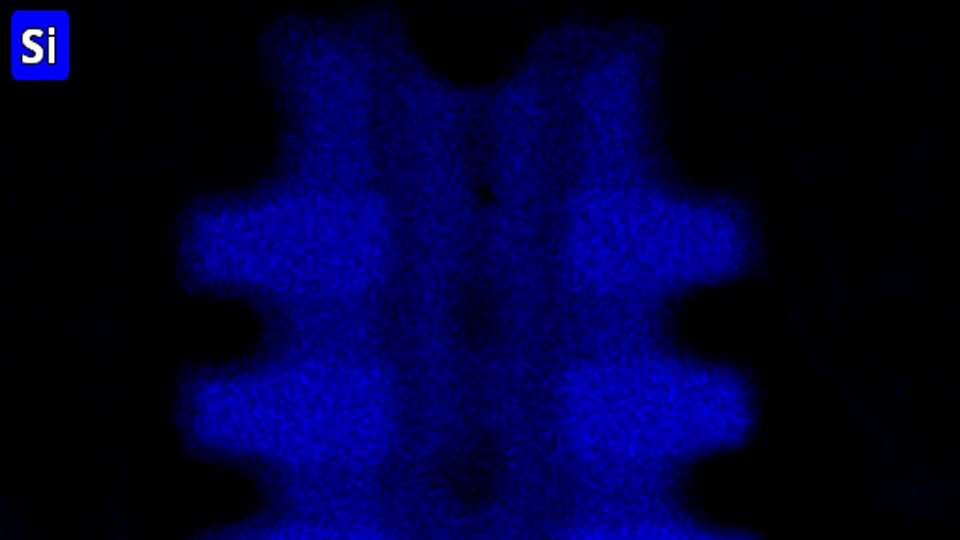
SEM imaging and EDS elemental analysis
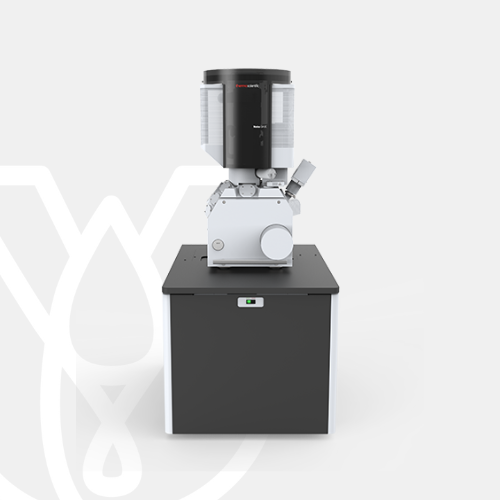
PT Wadya Prima Mulia as the Authorized Distributor for ThermoFisher Scientific in Indonesia, provides Verios 5 XHR Scanning Electron Microscope
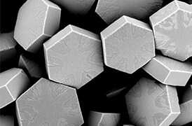
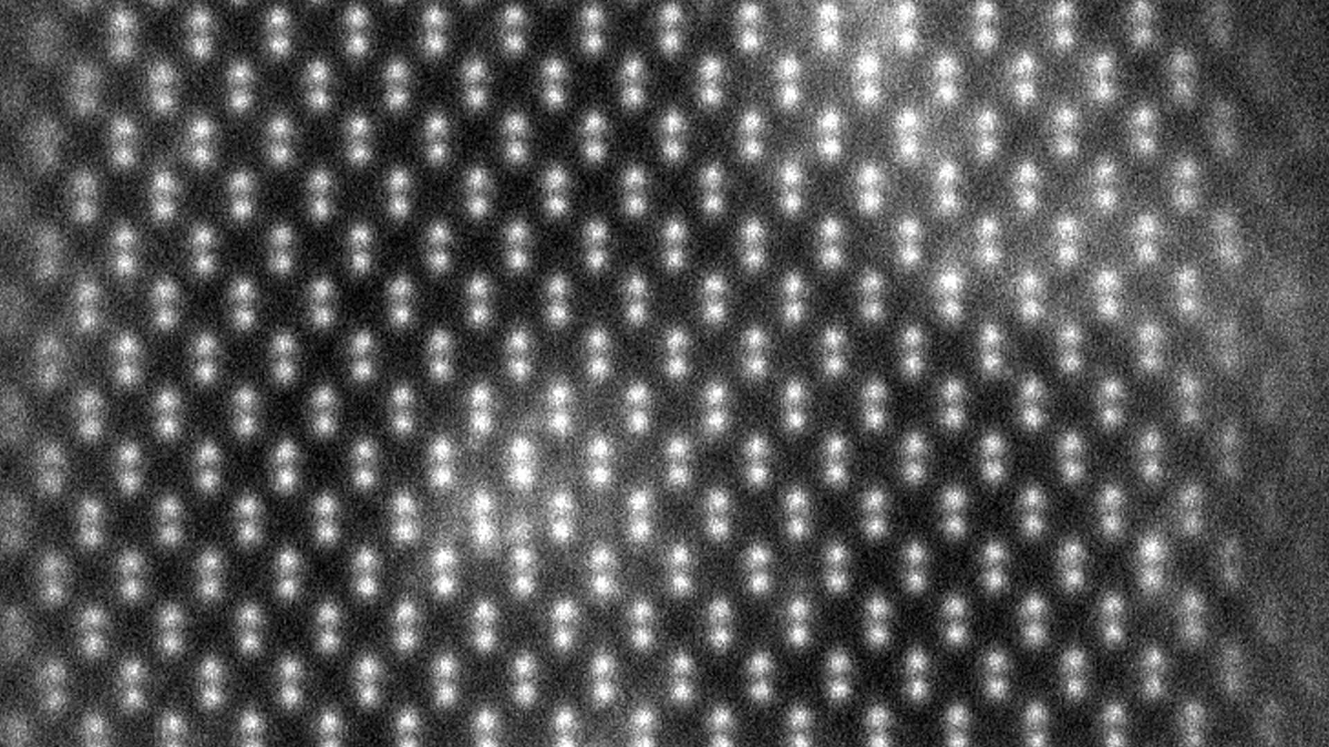
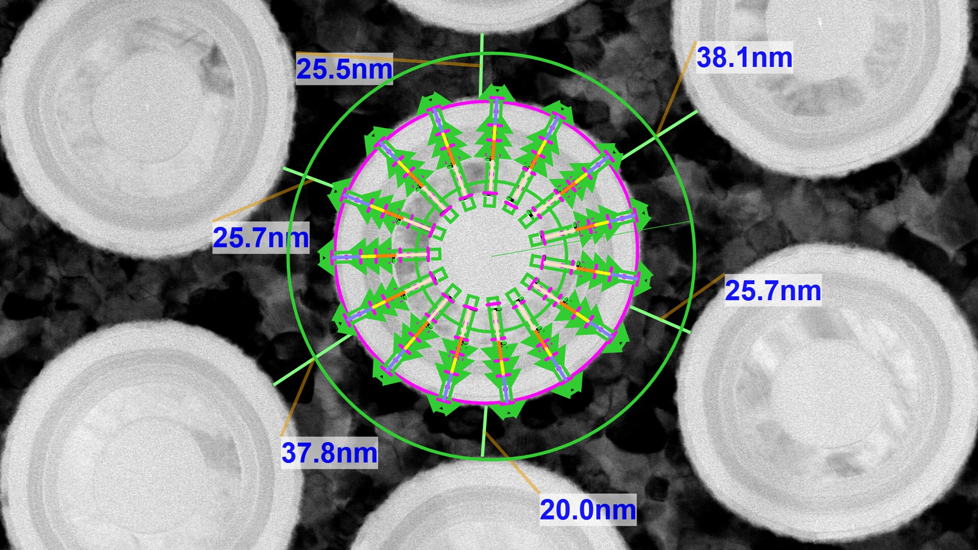
Scanning electron microscopy characterization of nanomaterials with sub-nanometer resolution and high material contrast.
For more information regarding the product, click here
Verios 5 XHR Scanning Electron Microscope
The Verios 5 XHR SEM offers subnanometer resolution over the full 1 keV to 30 keV energy range with excellent materials contrast. Unprecedented levels of automation and ease-of-use make this performance accessible to users of any experience level.
Scanning electron microscopy characterization
- High resolution nanomaterial imaging with the UC+ monochromated electron source for sub-nanometer performance from 1-30 kV.
- High contrast on sensitive materials with excellent performance down to 20 eV landing energy and high-sensitivity in-column and below-the-lens detectors and signal filtering for low-dose operation and optimal contrast selection.
- Greatly reduced time to nanoscale information for users with any experience level using the Elstar electron column featuring SmartAlign and FLASH technologies.
- Consistent measurement results with ConstantPower lenses, electrostatic scanning and a choice of two piezoelectric stages.
- Flexibility for accessories with a large chamber.
- Unattended SEM operation with Thermo Scientific AutoScript 4 Software, an optional Python-based application programming interface.
SmartAlign technology
SmartAlign technology eliminates the need for any user alignments of the electron column, which not only minimizes maintenance, but also increases your productivity.
Sub-nanometer resolution
Elstar Schottky monochromated (UC+) FESEM technology and performance with sub-nanometer resolution from 1 to 30 keV.
Low dose operation and optimal contrast selection
Advanced suite of high-sensitivity, in-column & below-the-lens detectors and signal filtering for low dose operation and optimal contrast selection.
Unattended SEM operation
Easily handle a wide range of applications, including insulating samples with Low Vac operation and advanced beam scanning to ensure high-fidelity imaging
Innovative electron optics
Including Thermo Scientific’s patented UC+ gun (monochromator), ConstantPower lenses and electrostatic scanning for accurate and stable imaging.
Consistent measurement results
The Verios is ideally suited to lab-based metrology applications, with the ability to calibrate to a NIST certified standard at high magnification.
Easy access to beam landing energies
As low as 20 eV with very high resolution for true surface characterization.
Large chamber
With a choice of two precise and stable piezo-driven stages.
| Electron beam resolution | • 0.6 nm at 30 kV STEM (optional) • 0.6 nm at 2-15 kV • 0.7 nm at 1 kV • 1.0 nm at 500 V |
| Standard detectors | ETD, TLD, MD, ICD, beam current measurement, Nav-Cam+, IR-camera |
| Optional detectors | Optional detectors | EDS, EBSD, RGB cathodoluminescence, Raman, WDS, and more |
| Stage bias (beam deceleration, optional) | Up to -4000 V, included as standard |
| Sample cleaning | Integrated plasma cleaner, included as standard |
| Sample manipulation | Verios 5 UC • 5-axis motorized eucentric stage, with XYR axes piezo driven. • XY range 150 x 150 mm2, 70° tilt range. • Loading through the door. Verios 5 HP • Chamber mounted, ultra-stable 5 axis all piezo motorized stage. • XY range 100 x 100 mm2, 70° tilt range. • Loading via automated load lock. |
| Chamber | 379 mm inside width, 21 ports |
| Software options | • Thermo Scientific Maps Software for automatic large area acquisition using tiling and stitching; correlative work • Thermo Scientific AutoScript 4 Software; a Python-based application programming interface • Pattern generation software • TopoMaps for image colorization, image analysis and 3D surface reconstruction |
Fundamental Materials Research
Novel materials are investigated at increasingly smaller scales for maximum control of their physical and chemical properties. Electron microscopy provides researchers with key insight into a wide variety of material characteristics at the micro- to nano-scale.
Semiconductor research and development
Innovation starts with research and development. Learn more about solutions to help you understand innovative structures and materials at the atomic level.
Semiconductor metrology
Manufacturing today’s complex semiconductors requires exact process controls. Learn more about advanced metrology and analysis solutions to accelerate yield learnings.
Semiconductor Failure Analysis
Complex semiconductor device structures result in more places for defects to hide. Learn more about failure analysis solutions to isolate, analyze, and repair defects.
Semiconductor materials characterization
Many factors impact yield, performance, and reliability. Learn more about solutions to characterize physical, structural, and chemical properties.
For other products from ThermoFisher, click here.