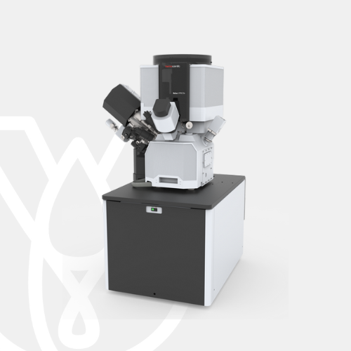
PT Wadya Prima Mulia as the Authorized Distributor for ThermoFisher Scientific in Indonesia, provides Helios 5 PFIB DualBeam
Plasma focused ion beam scanning electron microscope for TEM sample preparation including 3D characterization, cross-sectioning and micromachining.
For more information regarding the product, click here
Plasma focused ion beam instrument
The Thermo Scientific Helios 5 Plasma FIB (PFIB) DualBeam (focused ion beam scanning electron microscope, or FIB-SEM) delivers unmatched capabilities for materials science and semiconductor applications. For materials science researchers, the Helios 5 PFIB DualBeam provides large-volume 3D characterization, gallium-free sample preparation, and precise micromachining. For manufacturers of semiconductor devices, advanced packaging technology, and display devices, the Helios 5 PFIB DualBeam delivers damage-free, large-area de-processing, fast sample preparation, and high-fidelity failure analysis.
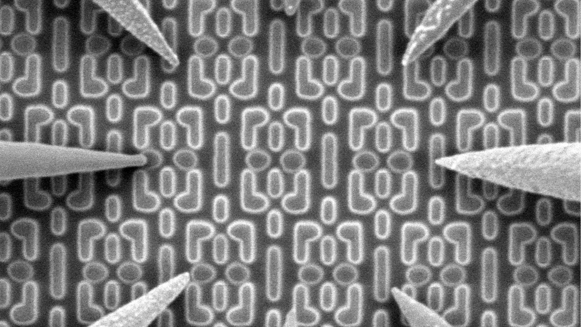
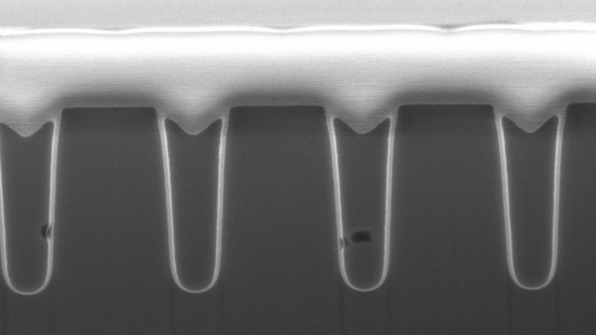
Gallium-free STEM and TEM sample preparation
High-quality, gallium-free TEM and APT sample preparation thanks to the new PFIB column enabling 500 V Xe+ final polishing and delivering superior performance at all operating conditions.
Advanced automation
Fastest and easiest, automated, multisite in situ and ex situ TEM sample preparation and cross-sectioning using optional AutoTEM 5 Software.
Next-generation 2.5 μA xenon plasma FIB column
High throughput and quality statistically relevant 3D characterization, cross-sectioning and micromachining using next generation 2.5 μA Xenon Plasma FIB column (PFIB).
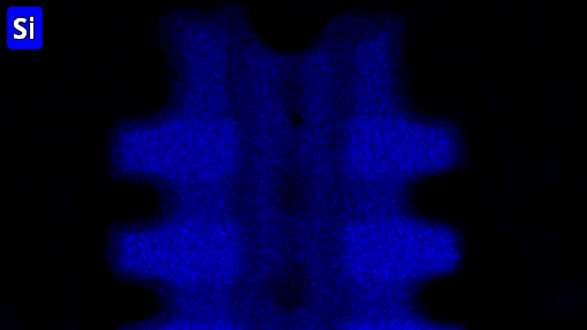
Multi-modal subsurface and 3D information
Access high-quality, multi-modal subsurface and 3D information with precise targeting of the region of interest using optional Auto Slice & View 4 (AS&V4) Software.
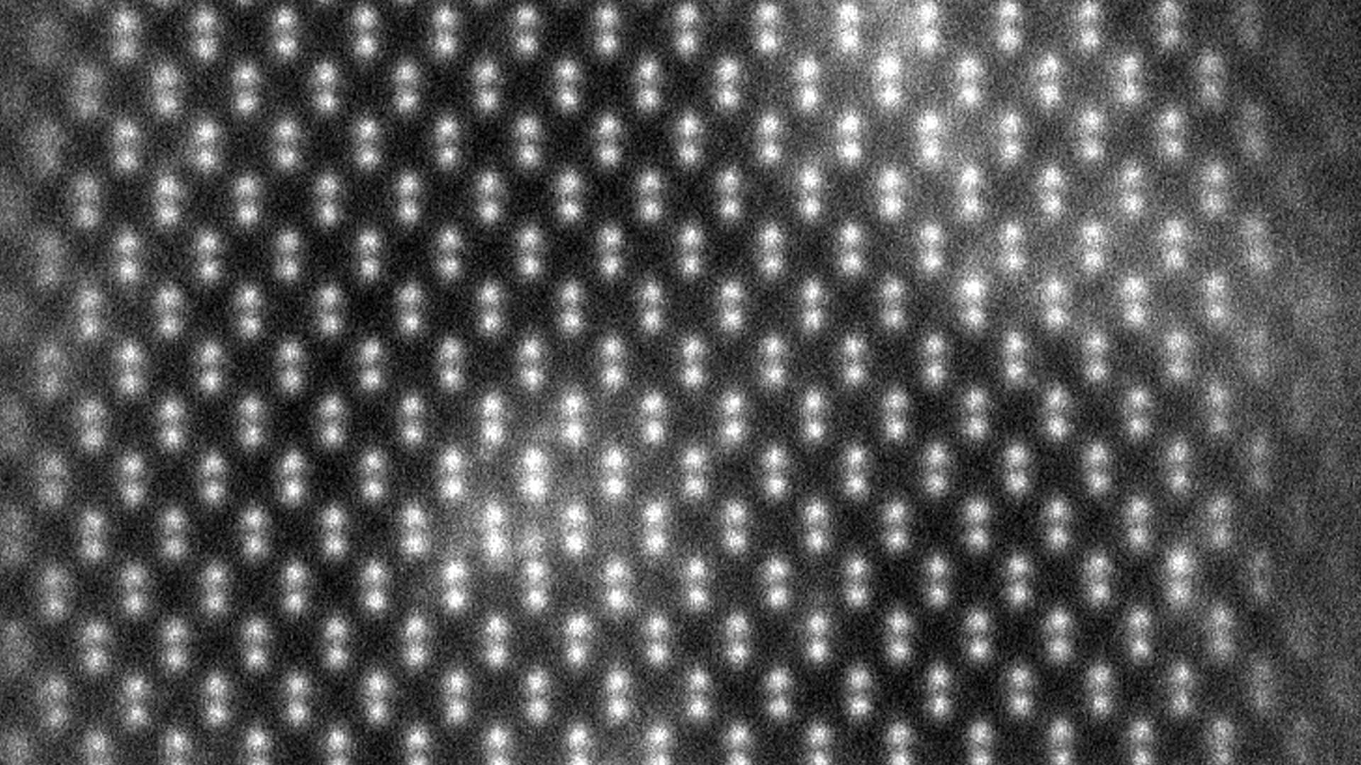
Sub-nanometer performance at low energies
Reveal the finest details using best-in-class Elstar Electron Column with high-current UC+ monochromator technology, enabling sub-nanometer performance at low energies.
Complete sample information
The most complete sample information with sharp, refined, and charge-free contrast obtained from up to six integrated in-column and below-the-lens detectors.
Advanced capabilities
Most advanced capabilities for electron and ion beam induced deposition and etching on FIB/SEM systems with optional Thermo Scientific MultiChem or GIS Gas Delivery Systems.
Artifact-free imaging
Artifact-free imaging based on integrated sample cleanliness management and dedicated imaging modes such as SmartScan™ and DCFI Modes.
Short time to nanoscale information
Shortest time to nanoscale information for users with any experience level with SmartAlign and FLASH technologies.
Precise sample navigation
Precise sample navigation tailored to individual application needs thanks to the high stability and accuracy of 150 mm Piezo stage and optional in-chamber Nav-Cam.
| Electron optics | Elstar extreme high-resolution field emission SEM column with: • Immersion magnetic objective lens • High-stability Schottky field emission gun to provide stable high-resolution analytical currents • UC+ monochromator technology |
| Electron beam resolution | At optimum working distance (WD): • 0.7 nm at 1 kV • 1.0 nm at 500 V (ICD) At coincident point:0.6 nm at 15 kV • 1.2 nm at 1 kV |
| Electron beam parameter space | • Electron beam current range: 0.8 pA to 100 nA • Accelerating voltage range: 200 V – 30 kV • Landing energy range: 20* eV – 30 keV • Maximum horizontal field width: 2.3 mm at 4 mm WD |
| Ion optics | High performance PFIB column with Inductively Coupled Xe+ Plasma (ICP)Ion beam current range: • 1.5 pA to 2.5 µA • Accelerating voltage range: 500 V – 30 kV • Maximum horizontal field width: 0.9mm at beam coincidence point Ion beam resolution at coincident point • <20 nm at 30 kV using preferred statistical method • <10 nm at 30 kV using selective edge method |
| Detectors | • Elstar in-lens SE/BSE detector (TLD-SE, TLD-BSE) • Elstar in-column SE/BSE detector (ICD)* • Everhart-Thornley SE detector (ETD) • IR camera for viewing sample/column • High-performance ion conversion and electron (ICE) detector for secondary ions (SI) and electrons (SE) • In-chamber Nav-Cam sample navigation camera* • Retractable low voltage, high contrast directional solid-state backscatter electron detector (DBS)* • Integrated beam current measurement |
| Stage and sample | Flexible 5-axis motorized stage: • XY range: 110 mm • Z range: 65 mm • Rotation: 360° (endless) • Tilt range: -38° to +90° • XY repeatability: 3 μm • Max sample height: Clearance 85 mm to eucentric point • Max sample weight at 0° tilt: 5 kg (including sample holder) • Max sample size: 110 mm with full rotation (larger samples possible with limited rotation) • Compucentric rotation and tilt |
Semiconductor Advanced Packaging
Performance, power efficiency, area, and cost are driving packaging innovations. Learn how workflows provide fast, precise, and accurate time-to-data.
Semiconductor Failure Analysis
Complex semiconductor device structures result in more places for defects to hide. Learn more about failure analysis solutions to isolate, analyze, and repair defects.
Semiconductor materials characterization
Many factors impact yield, performance, and reliability. Learn more about solutions to characterize physical, structural, and chemical properties.
Novel architectures and materials pose new challenges. Learn how to pinpoint faults and characterize materials, structures, and interfaces.
Semiconductor research and development
Innovation starts with research and development. Learn more about solutions to help you understand innovative structures and materials at the atomic level.

Semiconductor display technology
Display technologies are evolving to improve display quality and light conversion efficiency. Learn how metrology, failure analysis, and characterization solutions provide insights.
Process control using electron microscopy
Modern industry demands high throughput with superior quality, a balance that is maintained through robust process control. SEM and TEM tools with dedicated automation software provide rapid, multi-scale information for process monitoring and improvement.
Quality control and failure analysis
Quality control and assurance are essential in modern industry. We offer a range of EM and spectroscopy tools for multi-scale and multi-modal analysis of defects, allowing you to make reliable and informed decisions for process control and improvement.
Fundamental Materials Research
Novel materials are investigated at increasingly smaller scales for maximum control of their physical and chemical properties. Electron microscopy provides researchers with key insight into a wide variety of material characteristics at the micro- to nano-scale.
For other products from ThermoFisher, click here.