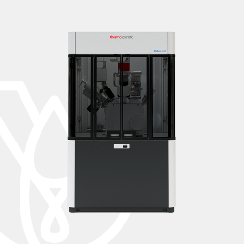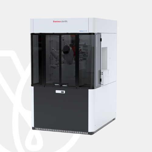
FIB SEM instruments for automated structural analysis, TEM sample preparation, and nano-prototyping.
Focused ion beam scanning electron microscopy
Scientists and engineers in both academia and industry are constantly facing new challenges that require highly localized characterization of a wide range of samples and materials. The ongoing drive to improve the quality of these materials means that structural and compositional information at the nanoscale is frequently necessary. FIB-SEM instruments generate exactly this kind of data by combining the precise sample modification of FIB with the high-resolution imaging of SEM.
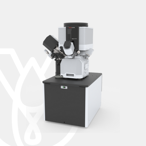
DualBeam instruments
Thermo Fisher Scientific is the industry leader in FIB-SEM technology with more than 30 years of experience with DualBeams. The technology’s novel ability to reveal subsurface structural detail, by making precise cuts with a FIB and then imaging the exposed surface with a high-resolution SEM, has led to its acceptance by researchers and engineers in a wide variety of applications. With more than 2,000 Thermo Scientific systems installed around the world, our DualBeams continue to lead the market with cutting-edge capabilities built on technical innovation and a deep store of application knowledge gathered over years of collaborative development with our customers.
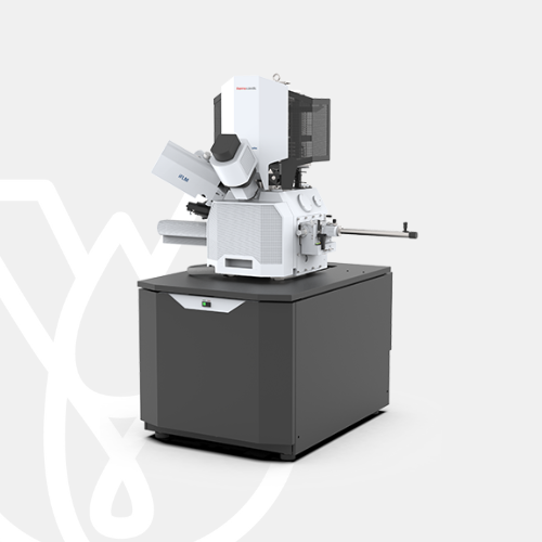
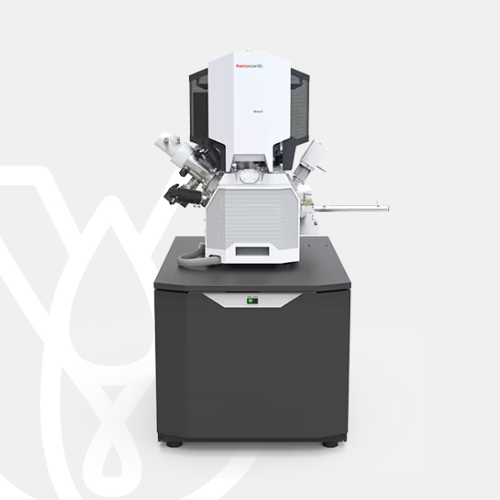
TriBeam instruments
The new TriBeam systems are our latest FIB-SEM innovation, featuring the addition of a femtosecond laser, which can cut many materials at rates that are orders of magnitude faster than a typical FIB. A large cross-section (hundreds of micrometers) can be created in less than five minutes. Because the laser has a different removal mechanism (ablation versus the ion sputtering of FIB), it can easily process challenging materials, such as non-conductive or ion-beam-sensitive samples. The extremely short duration of the femtosecond laser pulses introduces almost no artifacts such as heat impact, microcracking, melting, or those typical of traditional mechanical polishing. In most cases, the laser-milled surfaces are clean enough for direct SEM imaging and even for surface-sensitive techniques such as electron backscatter diffraction (EBSD) mapping.
We offer a broad product portfolio and advanced automation capabilities for applications such as transmission electron microscopy (TEM) sample preparation, subsurface and 3D characterization, nano-prototyping, and in situ experimentation.