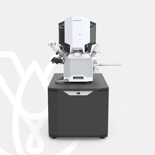
PT Wadya Prima Mulia as the Authorized Distributor for ThermoFisher Scientific in Indonesia, provides Scios 2 DualBeam
Focused ion beam scanning electron microscope for ultra-high resolution, high-quality sample preparation and 3D characterization.
For more information regarding the product, click here
Focused ion beam scanning electron microscopy
The Thermo Scientific Scios 2 DualBeam is an ultra-high-resolution analytical focused ion beam scanning electron microscopy (FIB-SEM) system that provides outstanding sample preparation and 3D characterization performance for a wide range of samples, including magnetic and non-conductive materials. With innovative features designed to increase throughput, precision, and ease of use, the Scios 2 DualBeam is an ideal solution to meet the needs of scientists and engineers in advanced research and analysis across academic, governmental, and industrial research environments.
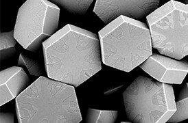
Subsurface characterization
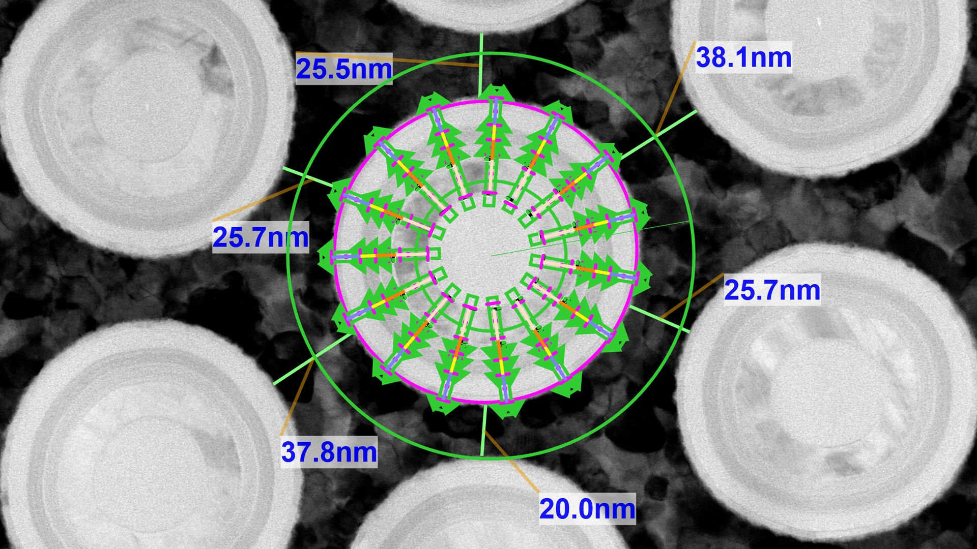
Subsurface or three-dimensional characterization is often required to better understand the structure and properties of a sample. The Scios 2 DualBeam, with optional Thermo Scientific Auto Slice & View 4 (AS&V4) Software, allows for high-quality, fully automated acquisition of multi-modal 3D datasets, including backscattered electron (BSE) imaging for maximum materials contrast, energy-dispersive spectroscopy (EDS) for compositional information, and electron backscatter diffraction (EBSD) for microstructural and crystallographic information. Combined with Thermo Scientific Avizo Software, the Scios 2 DualBeam delivers a unique workflow solution for high-resolution, advanced 3D characterization and analysis at the nanometer scale.
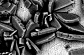
Backscattered electron and secondary electron imaging
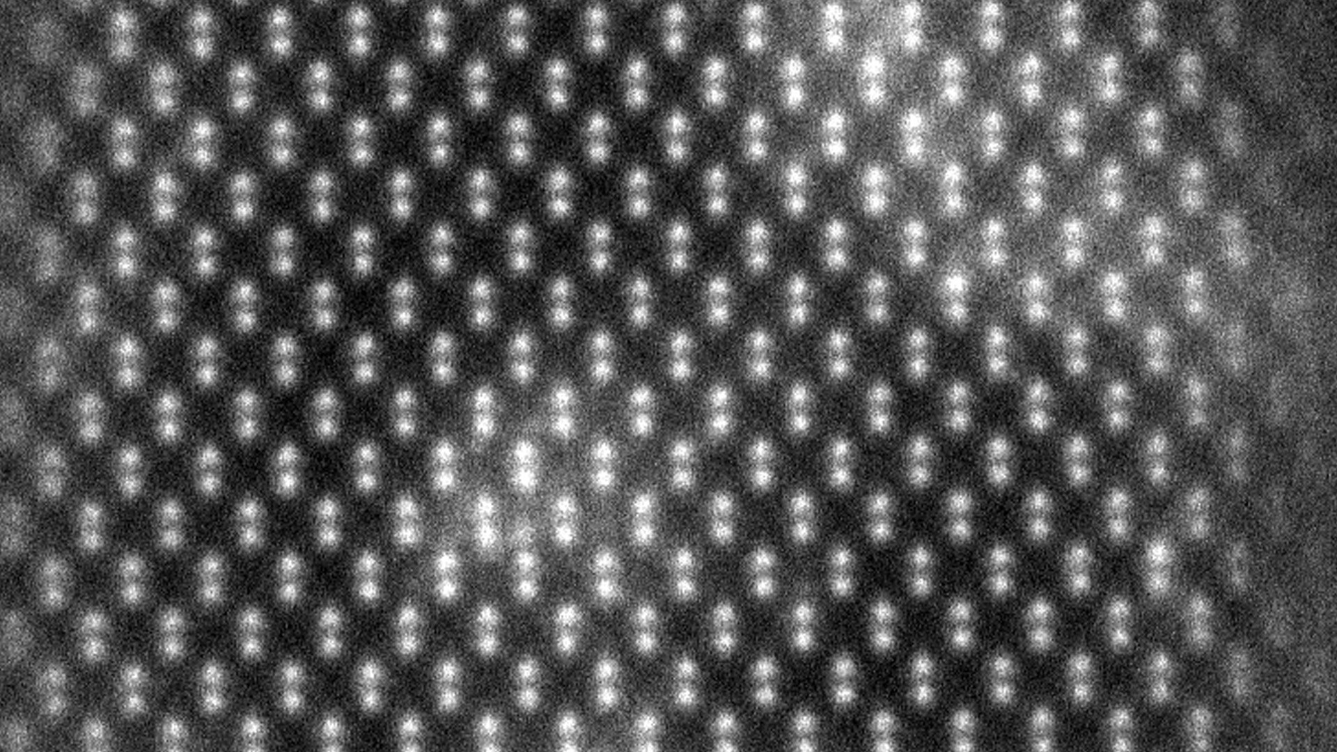
The innovative NICol electron column provides the foundation of the system’s high-resolution imaging and detection capabilities. It offers excellent nanoscale details, with a wide range of working conditions, whether operating at 30 keV in STEM mode (to access structural information) or at lower energies (to obtain charge-free, detailed surface information). With its unique in-lens Thermo Scientific Trinity Detection System, the Scios 2 DualBeam is designed for simultaneous acquisition of angular and energy-selective secondary electron (SE) and BSE imaging. Fast access to detailed nanoscale information is possible not only top-down, but also on tilted specimens or cross-sections. Optional below-the-lens detectors and an electron-beam-deceleration mode ensure fast and easy simultaneous collection of all signals, revealing the smallest features in a material surface or cross-section. Fast, accurate, and reproducible results are obtained thanks to the unique NICol column design with full auto alignments.
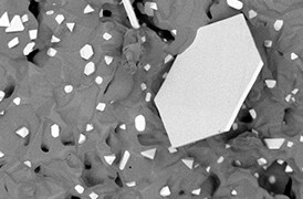
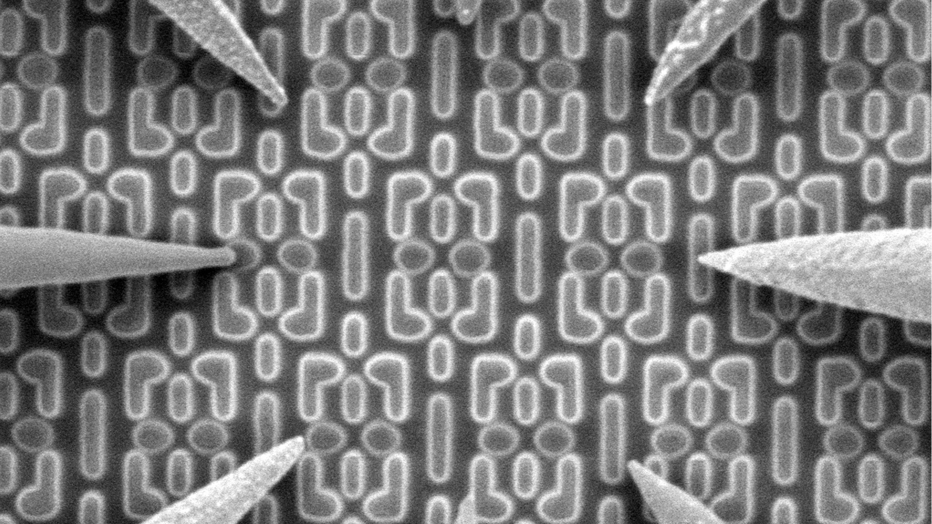
TEM sample preparation
Scientists and engineers constantly face new challenges that require highly localized characterization of increasingly complex samples with ever smaller features. The latest technological innovations of the Scios 2 DualBeam, in combination with the optional, easy-to-use, comprehensive Thermo Scientific AutoTEM 4 Software and Thermo Fisher Scientific’s application expertise, allow for fast and easy preparation of site-specific high-resolution S/TEM samples for a wide range of materials. In order to achieve high-quality results, final polishing with low-energy ions is required to minimize surface damage on the sample. The Thermo Scientific Sidewinder HT Focused Ion Beam (FIB) column not only delivers high-resolution imaging and milling at high voltages but also offers good low-voltage performance, enabling the creation of high-quality TEM lamella.
Fast and easy preparation
High-quality, site-specific, TEM and atom probe samples using the Sidewinder HT ion column.
Ultra-high resolution imaging
Using the Thermo Scientific NICol Electron Column with best-in-class performance on the widest range of samples, including magnetic and nonconductive materials.
The most complete sample information
With sharp, refined, and charge-free contrast obtained from a variety of integrated in-column and below-the-lens detectors.
High-quality, multi-modal subsurface and 3D information
Access the high-quality, multi-modal subsurface and 3D information with precise targeting of the region of interest using optional AS&V4 Software.
Precise sample navigation
Tailored to individual application needs thanks to the high flexibility 110 mm stage and in-chamber Thermo Scientific Nav-Cam Camera.
Artifact-free imaging and patterning
With dedicated modes such as DCFI, drift suppression and Thermo Scientific SmartScan Modes.
Optimize your solution
Meet specific application requirements thanks to flexible DualBeam configuration, including optional low-vacuum mode with up to 500 Pa chamber pressure.
| Electron beam resolution | • Optimum WD • 0.7 nm at 30 keV STEM • 1.4 nm at 1 keV • 1.2 nm at 1 keV with beam deceleration |
| Electron beam parameter space | • Beam current range: 1 pA to 400 nA • Landing energy range: 20* eV – 30 keV • Accelerating voltage range: 200 V – 30 kV • Maximum horizontal field width: 3.0 mm at 7 mm WD and 7.0 mm at 60 mm WD • Extra wide field of view (1×) available through standard navigation montage |
| Ion optics | • Acceleration voltage: 500 V – 30 kV • Beam current range: 1.5 pA – 65 nA • 15-position aperture strip • Drift suppression mode as standard for non-conductive samples • Minimum source lifetime: 1,000 hours • Ion beam resolution: 3.0 nm at 30kV using selective edge method |
| Detectors | • Trinity Detection System (in-lens and in-column) • T1 segmented lower in-lens detector • T2 upper in-lens detector • T3 retractable in-column detector (Optional) • Up to four simultaneously detected signals • Everhart-Thornley SE Detector (ETD) • High-performance ion conversion and electron (ICE) detector for secondary ions (SI) and electrons (SE) (Optional) • Retractable low-voltage, high-contrast, segmented solid-state backscatter electron detector (DBS) (Optional) • Retractable STEM 3+ detector with BF/ DF/ HAADF segments (Optional) • IR camera for viewing sample and chamber • In-chamber Nav-Cam sample navigation camera (Optional) • Integrated beam current measurement |
| Stage and sample | Flexible 5-axis motorized stage: • XY range: 110 mm • Z range: 65 mm • Rotation: 360° (endless) • Tilt range: -15° to +90° • XY repeatability: 3 μm • Max sample height: Clearance 85 mm to eucentric point • Max sample weight at 0° tilt: 5 kg (including sample holder) • Max sample size: 110 mm with full rotation (larger sample possible with limited rotation) • Compucentric rotation and tilt |
Process control using electron microscopy
Modern industry demands high throughput with superior quality, a balance that is maintained through robust process control. SEM and TEM tools with dedicated automation software provide rapid, multi-scale information for process monitoring and improvement.
Quality control and failure analysis
Quality control and assurance are essential in modern industry. We offer a range of EM and spectroscopy tools for multi-scale and multi-modal analysis of defects, allowing you to make reliable and informed decisions for process control and improvement.
Fundamental Materials Research
Novel materials are investigated at increasingly smaller scales for maximum control of their physical and chemical properties. Electron microscopy provides researchers with key insight into a wide variety of material characteristics at the micro- to nano-scale.
Semiconductor research and development
Innovation starts with research and development. Learn more about solutions to help you understand innovative structures and materials at the atomic level.
Manufacturing today’s complex semiconductors requires exact process controls. Learn more about advanced metrology and analysis solutions to accelerate yield learnings.
Semiconductor Failure Analysis
Complex semiconductor device structures result in more places for defects to hide. Learn more about failure analysis solutions to isolate, analyze, and repair defects.
Semiconductor materials characterization
Many factors impact yield, performance, and reliability. Learn more about solutions to characterize physical, structural, and chemical properties.
For other products from ThermoFisher, click here.